
|
While stress is a bad thing in our day to day lives, stress in materials can be exploited to achieve useful properties. For instance, computer processors have become faster and faster over the last few decades exploiting stress in semiconductor materials. The stress causes the charge carriers to have a lower effective mass and this, in turn, increases their mobility. This increases the clock speed of the computer processors. As our laptop becomes old, the semiconductor material “gets tired” of the stress (so to speak) and the atoms start rearranging themselves to lower the stress. The increased carrier mobility is lost and the effect is seen in the laptop speed, which starts to slow down. Epitaxially grown films are those that are grown directly on top of a base (called a substrate) using a fabrication method like Chemical Vapor Deposition (CVD) or Physical Vapor Deposition (PVD) or Atomic Layer Deposition (ALD) or Molecular Beam Epitaxy (MBE) or any of their variants. All materials have a favorite interatomic distance that is energetically most suitable. This distance is referred to as the lattice constant. If the lattice constant of the substrate matches that of the material being deposited on top of it, atoms can neatly form a layer on top of the substrate. However, often, there is a mismatch in the lattice constants of the substrate and the material on top. As shown in Figure 1, when the lattice constant of the thin film at the top is greater than that of the substrate, the atoms of the film have to be squeezed so that they can sit on top of the substrate. Similarly, when the lattice constant of the thin film at the top is smaller than that of the substrate, the atoms of the film have to be pulled apart so that they can sit on top of the substrate. This causes compressive and tensile stress respectively.  Fig. 1: Compressive and tensile stress (Source: Semiconductor Engg. Jour. 2017). A typical E-k plot (Energy vs Reciprocal space vector) of semiconductor materials looks like this. Notice the plot for the hole is less steep than that of the electron. 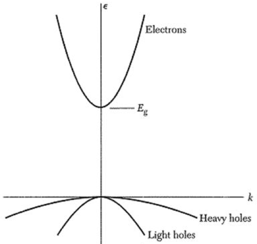 Fig. 2: E-k plot of a typical semiconductor material (Source: Kittel 8th Ed). The effective mass of a charge carrier is given by this equation below. Here the denominator is the curvature of the E-k plot.  The higher the curvature is, the lower the effective mass is and the faster the carriers can travel. This explains why electrons have a higher mobility than holes do. By engineering a stress, the curvature can be made steeper, thereby increasing mobility. The measurement of stress in material becomes crucial in design and research of this technique. Stress affects the vibration modes of the atoms and this causes a shift in the Raman spectrum. Hence, Raman spectroscopy is often used to ascertain the stress level in material.  Fig. 3: Raman spectrum shift with stress (Source: www.nanophoton.net). So next time your phone or laptop slows down as it gets older, don’t assume that the vendor has deliberately done this to force an upgrade. Often, it’s due to the way the faster speed was achieved in the first place!
1 Comment
2/5/2019 10:40:25 am
Youre so cool! I don’t suppose I’ve read anything like this before. So nice to find somebody with some original thoughts on this subject. really thank you for starting this up. this website is something that is needed on the web, someone with a little originality. useful job for bringing something new to the internet! Leave a Reply. |
About the Author(S)The contributors to this blog are the students, faculty, and other researchers in the Department of Physics & Astronomy at Northern Arizona University. If you have any suggestions, or would like to contribute to this blog, please email mark.salvatore@nau.edu for more information. Archives
January 2019
Categories |
 RSS Feed
Site powered by Weebly. Managed by Bluehost